Introduction
Antifuse one-time programmable (OTP) is the most secure embedded non-volatile memory (eNVM). The default value is 1 and can only be change from 1 to 0.

OTP Layout
Note
For detailed layout of each OTP zone, refer to UM1000.
OTP Programming APIs
API |
Description |
Operation zone |
|---|---|---|
OTP_Read8 |
Read OTP physical zone one byte |
Physical zone |
OTP_Write8 |
Write OTP physical zone one byte |
Physical zone |
OTP_LogicalMap_Read |
Read OTP logical zone by length |
Logical zone |
OTP_LogicalMap_Write |
Write OTP logical address by length |
Logical zone |
OTP_RemainLength |
Get OTP remain available length used for logical map |
Logical zone |
OTPGetCRC |
Get the CRC of security area |
Physical zone |
OTP_Read8
Items |
Description |
|---|---|
Introduction |
Read OTP physical zone one byte |
Parameters |
|
Return |
Result of read operation
|
OTP_Write8
Items |
Description |
|---|---|
Introduction |
Write OTP physical zone one byte |
Parameters |
|
Return |
Result of write operation
|
OTP_LogicalMap_Read
Items |
Description |
|---|---|
Introduction |
Read OTP logical map |
Parameters |
|
Return |
Result of read operation
|
OTP_LogicalMap_Write
Items |
Description |
|---|---|
Introduction |
Write OTP logical address by length |
Parameters |
|
Return |
Result of write operation
|
OTP_RemainLength
Items |
Description |
|---|---|
Introduction |
Get OTP remain available length used for logical map |
Parameters |
None |
Return |
Remain available length |
OTPGetCRC
Items |
Description |
|---|---|
Introduction |
Get the CRC value of security area |
Parameters |
None |
Return |
CRC value |
OTP Programming Commands
You can access OTP by the following commands from serial port.
Logical Zone
You can read and write the logical zone by commands listed below.
Operation |
Command |
Description |
|---|---|---|
Read |
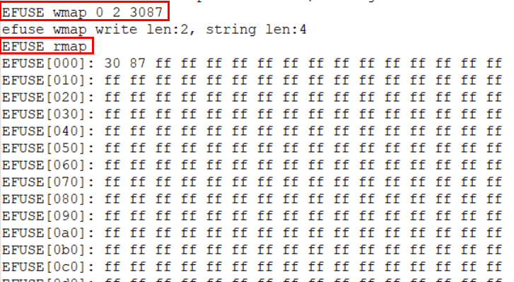
EFUSE rmap |
Read the whole logical zone. |
Write |
EFUSE wmap <address> <length> <data> |
Write to specific address of logical zone.
Note The string length of data to be written must be even. |
For example:
By command
EFUSE wmap 0 2 3087, you can write 0x3087 that is 2 bytes into logical address 0x0.By command
EFUSE rmap, the logical zone is all shown immediately.
In the massive production (MP) stage, another command to program logical zone is “iwpriv”, which has been integrated into RF calibration tools. This command is only recommended to be used to program Wi-Fi calibration zone.
Physical Zone
You can read and write the physical zone by commands listed below. The value of physical zone can only be written from 1 to 0, please program it carefully.
Operation |
Command |
Description |
|---|---|---|
Read |
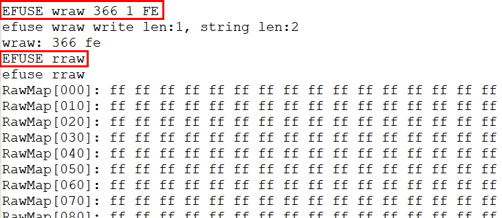
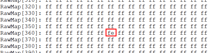
EFUSE rraw |
Read the whole physical zone. |
Write |
EFUSE wraw <address> <length> <data> |
Write to specific address of physical zone.
Note The string length of data to be written must be even. |
For example:
By command
FUSE wraw 366 1 FE, you can write 0xFE that is 1 byte into physical address 0x366 to enable theNS_IPSEC_Key2_R_Forbidden_ENbit.By command
EFUSE rraw, the physical zone is all shown immediately.
…
In the MP stage, you can also use Wi-Fi command iwpriv as mentioned in Logical Zone.
Usage
Logical Zone
The OTP can only be programmed once, however some data needs to be overwritten in some reason. Therefore, the logical data can be overwritten after format conversion defined by Realtek, as described in User Manual (Section: Mapping Relationship of Physical OTP and Logical OTP).
The logical zone can be programmed multi-times, in case the remain length of physical zone 0x0~0x1FF is enough.
Note
The logical zone is programmed in bytes instead of bits. Therefore, to avoid writing incorrectly that would cause wasting the physical zone for logical mapping, you should read logical map to check the original value before programming new value.
System Data
The logical area 0x000 ~ 0x01F (32 bytes) will be auto-loaded to system registers by hardware when the system boots. If the system data hasn’t been programmed, system registers keep initial value that are 0x00, however reading logical map will get 0xFF.
The procedure of programming the system data is described below.

Programming the system data
About the target address that you want to program, there’re two cases:
One is that the system data in the target address has been programmed before. In this case, you can refer to Example 1.
The other is that the system data hasn’t been programmed never. In this case, you can refer to Example 2.
Note
When programming the system data, the start address must be 4-byte aligned at 4-byte length.
Example 1
Program the value of logical address 0x02[1] to 1, you should follow these steps:
Read the logical map to check the original value in logical address 0x00~0x03.
efuse rmap
Or
u8 data_read[4];
OTP_LogicalMap_Read(&data_read,0,4);
Assume the data is 0x12A03456 in logical address 0x00~0x03 in Step 1. Let 0xA0 makes ‘OR’ operation with programmed bit[1], and other data keeps default value. So the new value to be written is 0x12A23456.
Write the new value 0x12A23456 to logical address 0x00~0x03.
efuse wmap 0 4 5634A212
Or
u8 data_written[4]={0x56,0x34,0xA2,0x12};
OTP_LogicalMap_Write(0,4,(u8 *)data_written);
Read the data_written again to check whether the value is written correctly.
efuse rmap
Or
u8 data_read[4];
OTP_LogicalMap_Read(&data_read,0,4);
Example 2
Program the value of logical address 0x08[0] to 1, you should follow following steps:
Read the logical map to check the original value.
efuse rmap
Or
u8 data_read[4];
OTP_LogicalMap_Read(&data_read,8,4);
Assume the data is 0xFFFFFFFF in logical address 0x08~0x0B in Step 1. Let 0x00 makes ‘OR’ operation with programmed bit[0], and other data keeps default value. So the new value to be written is 0x00000001.
Write the new value 0x00000001 to logical address 0x08~0x0B.
efuse wmap 8 4 01000000
Or
u8 data_written[4]={0x01,0x00,0x00,0x00};
OTP_LogicalMap_Write(8,4,(u8 *)data_written);
Read the data_written again to check whether the value is written correctly.
efuse rmap
Or
u8 data_read[4];
OTP_LogicalMap_Read(&data_read,8,4);
Wi-Fi Calibration Data
For detailed information about Wi-Fi Calibration Data, refer to WS_MP_FLOW.pdf.
Programming Scenarios
Usually, system data has their initial value, and you can program specific bits according to your demands. Table below lists some scenarios that specific bits need to be programmed at your requirements.
Offset |
Bit |
Symbol |
INI |
Description |
Scenarios |
|---|---|---|---|---|---|
0x02 |
[1] |
SPIC_ADDR_4BYTE_EN |
0 |
SPI Flash controller address 4-byte enable 0: Disable 1: Enable |
|
0x03 |
[1] |
LOW_BAUD_LOG_EN |
0 |
LOGUART baud rate selection 0: 1.5Mbps 1: 115200bps |
If the LOGUART baud rate needs to be changed from 1.5Mbps to 115200bps, program it. |
0x03 |
[0] |
DIS_BOOT_LOG_EN |
0 |
Boot ROM log disable 0: Enable 1: Disable |
If boot ROM log needs to be disabled, program it. |
Security Zone
The security zone is divided into three parts, as illustrated below.
Key area: 0x200~0x35F
Configuration area: 0x360~0x37F
User-defined area: 0x380~0x3FF

Security area layout
Key Area
Contents in key area are listed below. For more detailed usage about the keys, refer to the corresponding chapters:
Configuration Area
Contents in configuration area are listed below. About field’s usage in this area, you can get detailed information in the corresponding chapters.
CRC
CRC is used for defending against injection attacks, and this function is accomplished by comparing the valid CRC entry that you programmed into OTP with the one calculated by hardware for security zone (0x200~0x36B). If you want to ensure the secure zone un-attacked, then CRC field needs to be programmed.
One CRC entry takes 4 bytes, including a 2-byte magic number and a 2-byte valid CRC value.
There are 4 CRC entries in total in physical OTP and you can only use one entry at one time. You must use entry 0 first, and then entry1, entry2 and use entry3 at last. CRC check cannot be disabled once enabled. Rom will enter endless loop if magic number or valid CRC check fail.
When you use CRC validation function for the first time, please follow the following steps:
Program CRC entry after you make sure that security zone has been programmed done. Because any modification for the security zone (0x200~0x36B) will cause CRC value changed, then you have to re-program an new CRC entry, which will result in wasting one CRC entry
Get the valid CRC value without actually enabling the CRC function by func:
u32 OTPGetCRC(void)
Program valid CRC value calculated in previous step and magic number (0x8730) of the entry 0.
Magic number is 0x8730:
EFUSE wraw 370 2 3087
Assuming that CRC value is 0xB4C5:
EFUSE wraw 372 2 C5B4
Read the CRC entry back, to check whether it’s been written correctly
EFUSE rraw
Caution
Pay attention to the order of data.
Reset the chip
If the CRC entry is checked pass, the boot process will be successfully.
If the CRC entry is checked fail, the following log will show up, and the chip enters endless loop.
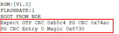
If security zone (0x200~0x36B) has been changed, a new CRC entry is needed.
Make sure that security zone has programmed done.
Get the new CRC value.
u32 OTPGetCRC(void)
Program the previous used entry to all 0x00 to invalidate this entry, that means both CRC and magic number are programmed into 0x00.
For example, assuming entry 0 is the previous entry:
EFUSE wraw 370 4 00000000
Program the next CRC entry with valid CRC and magic number to validate the next entry.
For example, if entry 0 is the previous entry, entry 1 should be used now:
Magic number is 0x8730:
EFUSE wraw 374 2 3087
Assuming that CRC value is 0xB4C5:
EFUSE wraw 376 2 C5B4
Read the CRC entry back to check whether it’s been written correctly
EFUSE rraw
Reset the chip to check if CRC entry is ok.
Caution
We suggest users programming CRC entry in factory.
Once CRC entry is programmed, and you need to modify secure zone. Please remember to invalidate current CRC entry and program the correct CRC value and magic number in the next CRC entry before re-boot. Otherwise, chip will enter endless loop and cannot boot successfully again.