概述
反熔丝一次性可编程存储器(One-Time Programmable, OTP) 是安全性最高的嵌入式非易失性存储器(eNVM)。其默认值为 1,且仅支持从 1 改写为 0。

OTP 布局
备注
关于 OTP 各分区的详细布局,请参考相应的 User Manual 文档。
OTP API 参考
API |
描述 |
操作区域 |
|---|---|---|
OTP_Read8 |
读取 OTP 物理区域单个字节 |
物理区域 |
OTP_Write8 |
写入 OTP 物理区域单个字节 |
物理区域 |
OTP_LogicalMap_Read |
按长度读取 OTP 逻辑映射区域 |
逻辑区域 |
OTP_LogicalMap_Write |
按长度写入 OTP 逻辑映射区域地址 |
逻辑区域 |
OTP_RemainLength |
获取逻辑映射区域中 OTP 剩余可用长度 |
逻辑区域 |
OTPGetCRC |
获取安全区域的 CRC 校验值 |
物理区域 |
OTP_Read8
项目 |
描述 |
|---|---|
功能 |
读取 OTP 物理区域单个字节 |
参数 |
|
返回值 |
读操作结果
|
OTP_Write8
项目 |
描述 |
|---|---|
功能 |
写入 OTP 物理区域单个字节 |
参数 |
|
返回值 |
写操作结果
|
OTP_LogicalMap_Read
项目 |
描述 |
|---|---|
功能 |
按长度读取 OTP 逻辑映射区域 |
参数 |
|
返回值 |
读操作结果
|
OTP_LogicalMap_Write
项目 |
描述 |
|---|---|
功能 |
按长度写入 OTP 逻辑映射区域地址 |
参数 |
|
返回值 |
写操作结果
|
OTP_RemainLength
项目 |
描述 |
|---|---|
功能 |
获取逻辑映射区域中 OTP 剩余可用长度 |
参数 |
无 |
返回值 |
剩余可用长度 |
OTPGetCRC
项目 |
描述 |
|---|---|
功能 |
获取安全区域的 CRC 校验值 |
参数 |
无 |
返回值 |
CRC 校验值 |
OTP 编程命令
可通过串口使用以下命令访问 OTP 的物理区域和逻辑区域:
逻辑区域
通过以下命令可以对逻辑区域进行读写操作。
操作 |
命令 |
描述 |
|---|---|---|
读 |
EFUSE rmap |
读取整个逻辑区域 |
写 |
EFUSE wmap <address> <length> <data> |
写入到逻辑区域的指定地址
备注 待写入数据的字符串长度必须为偶数。 |
例如:
通过命令
EFUSE wmap 0 2 3087可以将 0x3087 (2字节)写入逻辑映射地址 0x0。通过命令
EFUSE rmap可以立即读取整个逻辑区域。
EFUSE wmap 0 2 3087
efuse wmap write len:2, string len:4
EFUSE rmap
EFUSE[000]: 30 87 ff ff ff ff ff ff ff ff ff ff ff ff ff ff
EFUSE[010]: ff ff ff ff ff ff ff ff ff ff ff ff ff ff ff ff
EFUSE[020]: ff ff ff ff ff ff ff ff ff ff ff ff ff ff ff ff
EFUSE[030]: ff ff ff ff ff ff ff ff ff ff ff ff ff ff ff ff
...
在大批量生产(MP)阶段,可通过另一个命令 iwpriv 操作逻辑区域。这个命令已经集成在 RF 校准工具中,但仅推荐用来操作 Wi-Fi 校准区域。
物理区域
通过以下命令可以对物理区域进行读写操作。物理区域的值仅支持从 1 改写为 0,请谨慎操作。
操作 |
命令 |
描述 |
|---|---|---|
读 |
EFUSE rraw |
读取整个物理区域 |
写 |
EFUSE wraw <address> <length> <data> |
写入到物理区域的指定地址
备注 待写入数据的字符串长度必须为偶数。 |
例如:
通过命令
EFUSE wraw 366 1 FE可以将 0xFE (1字节)写入物理地址 0x366,从而使能NS_IPSEC_Key2_R_Forbidden_EN位。通过命令
EFUSE rraw可以立即读取整个物理区域。
EFUSE wraw 366 1 FE
efuse wraw write len:1, string len:2
wraw: 366 fe
EFUSE rraw
efuse rraw
RawMap[000]: ff ff ff ff ff ff ff ff ff ff ff ff ff ff ff ff
RawMap[010]: ff ff ff ff ff ff ff ff ff ff ff ff ff ff ff ff
RawMap[020]: ff ff ff ff ff ff ff ff ff ff ff ff ff ff ff ff
RawMap[030]: ff ff ff ff ff ff ff ff ff ff ff ff ff ff ff ff
...
RawMap[340]: ff ff ff ff ff ff ff ff ff ff ff ff ff ff ff ff
RawMap[350]: ff ff ff ff ff ff ff ff ff ff ff ff ff ff ff ff
RawMap[360]: ff ff ff ff ff ff fe ff ff ff ff ff ff ff ff ff
RawMap[370]: ff ff ff ff ff ff ff ff ff ff ff ff ff ff ff ff
...
在大批量生产阶段,同样可以使用 Logical Zone 中提到的 Wi-Fi 命令 iwpriv。
使用方法
逻辑区域
OTP 仅能编程一次,但在某些情况下部分数据需要被重写。因此,经 Realtek 定义的格式转换后,可以支持逻辑数据被重写,具体请参阅用户手册。
若物理区域(0x0~0x1FF)的剩余空间足够,逻辑区域可被多次编程。
备注
逻辑区域按字节(而非按位)编程。因此,为避免错误写入导致逻辑映射占用不必要的物理区域,写入新值前应读取逻辑映射以检查原始值。
系统数据
逻辑区域(0x000 ~ 0x01F,32字节)会在系统启动时由硬件自动加载至系统寄存器。若系统数据未被编程,系统寄存器保持初始值 0x00,但读取逻辑映射将返回 0xFF。
系统数据的编程流程如下:

针对目标地址的编程分为两种情况:
备注
编程系统数据时,起始地址必须为 4 字节对齐,且长度为 4 字节。
示例 1
将逻辑地址 0x02[1] 的值编程为 1,按以下步骤操作:
读取逻辑映射,检查逻辑地址 0x00~0x03 的原始值。
efuse rmap
或
u8 data_read[4];
OTP_LogicalMap_Read(&data_read,0,4);
假设步骤 1 中读取的逻辑地址 0x00~0x03 数据为 0x12A03456。将 0xA0`(地址 0x02 的字节)与目标位 [1] 进行或操作,其余数据保持默认值。所以新写入的值为 `0x12A23456。
写入新值 0x12A23456 到逻辑地址 0x00~0x03。
efuse wmap 0 4 5634A212
或
u8 data_written[4]={0x56,0x34,0xA2,0x12};
OTP_LogicalMap_Write(0,4,(u8 *)data_written);
再次读取数据以验证写入是否成功。
efuse rmap
或
u8 data_read[4];
OTP_LogicalMap_Read(&data_read,0,4);
示例 2
将逻辑地址 0x08[0] 的值编程为 1,按以下步骤操作:
读取逻辑映射,检查逻辑地址 0x08~0x0B 的原始值。
efuse rmap
或
u8 data_read[4];
OTP_LogicalMap_Read(&data_read,8,4);
假设步骤 1 中读取的逻辑地址 0x08~0x0B 数据为 0xFFFFFFFF。将 0x00`(地址 0x08 的字节)与目标位 [0] 进行或操作,其余数据保持默认值。所以新写入的值为 `x00000001。
写入新值 0x00000001 到逻辑地址 0x08~0x0B。
efuse wmap 8 4 01000000
或
u8 data_written[4]={0x01,0x00,0x00,0x00};
OTP_LogicalMap_Write(8,4,(u8 *)data_written);
再次读取数据以验证写入是否成功。
efuse rmap
或
u8 data_read[4];
OTP_LogicalMap_Read(&data_read,8,4);
Wi-Fi 校准数据
关于 Wi-Fi 校准数据的详细信息,请参考 WS_MP_FLOW.pdf。
编程场景
Usually, system data has their initial value, and you can program specific bits according to your demands. Table below lists some scenarios that specific bits need to be programmed at your requirements.
Offset |
Bit |
Symbol |
INI |
Description |
Scenarios |
|---|---|---|---|---|---|
0x02 |
[1] |
SPIC_ADDR_4BYTE_EN |
0 |
SPI Flash controller address 4-byte enable 0: Disable 1: Enable |
|
0x03 |
[1] |
LOW_BAUD_LOG_EN |
0 |
LOGUART baud rate selection 0: 1.5Mbps 1: 115200bps |
If the LOGUART baud rate needs to be changed from 1.5Mbps to 115200bps, program it. |
0x03 |
[0] |
DIS_BOOT_LOG_EN |
0 |
Boot ROM log disable 0: Enable 1: Disable |
If boot ROM log needs to be disabled, program it. |
Usually, system data has their initial value, and you can program specific bits according to your demands. Table below lists some scenarios that specific bits need to be programmed at your requirements.
Offset |
Bit |
Symbol |
INI |
Description |
Scenarios |
|---|---|---|---|---|---|
0x02 |
[1] |
SPIC_ADDR_4BYTE_EN |
0 |
SPI Flash controller address 4-byte enable 0: Disable 1: Enable |
|
0x02 |
[7] |
BIG_PAGE_NAND |
0 |
NAND Flash page 0: 2K 1: 4K |
|
0x03 |
[1] |
LOW_BAUD_LOG_EN |
0 |
LOGUART baud rate selection 0: 1.5Mbps 1: 115200bps |
If the LOGUART baud rate needs to be changed from 1.5Mbps to 115200bps, program it. |
0x03 |
[0] |
DIS_BOOT_LOG_EN |
0 |
Boot ROM log disable 0: Enable 1: Disable |
If boot ROM log needs to be disabled, program it. |
安全区域
安全区域分为以下三个部分:
密钥区域:0x200~0x35F
配置区域:0x360~0x37F
用户自定义区域:0x380~0x3FF

密钥区域
密钥区域包括以下内容,请至相应的章节查看各密钥的具体用法。
IPSEC:参考 对称硬件加密引擎
RSIP:参考 RSIP
SWD:参考 SWD 保护
PSA:参考 HUK 生成
安全启动:参考 安全启动
Function |
Name |
Size (bits) |
Start offset |
End offset |
|---|---|---|---|---|
IPSEC |
S_IPSEC_Key1 (RDP) |
256 |
0x200 |
0x021F |
IPSEC |
S_IPSEC_Key2 (Secure boot HMAC) |
256 |
0x220 |
0x023F |
IPSEC |
NS_IPSEC_Key1 |
256 |
0x240 |
0x025F |
IPSEC |
NS_IPSEC_Key2 |
256 |
0x260 |
0x027F |
USER PRI |
USER_PRI_KEY1 |
256 |
0x280 |
0x029F |
USER PRI |
USER_PRI_KEY2 |
256 |
0x2A0 |
0x02BF |
RSIP |
RSIP_KEY1 |
256 |
0x2C0 |
0x02DF |
RSIP |
RSIP_KEY2 |
256 |
0x2E0 |
0x02FF |
SWD |
SWD_PASSWORD |
128 |
0x300 |
0x030F |
PSA |
HUK |
128 |
0x310 |
0x031F |
Secure Boot |
PK1 (ROTPK hash) |
256 |
0x320 |
0x033F |
Secure Boot |
PK2 (ROTPK hash) |
256 |
0x340 |
0x035F |
Function |
Name |
Size (bits) |
Start offset |
End offset |
|---|---|---|---|---|
IPSEC |
S_IPSEC_Key1 (RDP) |
256 |
0x200 |
0x021F |
S_IPSEC_Key2 (Secure boot HMAC) |
256 |
0x220 |
0x023F |
|
NS_IPSEC_Key1 |
256 |
0x240 |
0x025F |
|
NS_IPSEC_Key2 |
256 |
0x260 |
0x027F |
|
ECDSA |
ECDSA_PRI_KEY1 |
256 |
0x280 |
0x029F |
ECDSA_PRI_KEY2 |
256 |
0x2A0 |
0x02BF |
|
RSIP |
RSIP_KEY1 |
256 |
0x2C0 |
0x02DF |
RSIP_KEY2 |
256 |
0x2E0 |
0x02FF |
|
SWD |
SWD_PASSWORD |
128 |
0x300 |
0x030F |
PSA |
HUK |
128 |
0x310 |
0x031F |
Secure Boot |
PK1 (ROTPK hash) |
256 |
0x320 |
0x033F |
PK2 (ROTPK hash) |
256 |
0x340 |
0x035F |
Function |
Name |
Size (bits) |
Start offset |
End offset |
Usage |
|---|---|---|---|---|---|
IPSEC |
S_IPSEC_Key1 (RDP) |
256 |
0x200 |
0x021F |
|
S_IPSEC_Key2 (Secure boot HMAC) |
256 |
0x220 |
0x023F |
||
NS_IPSEC_Key1 |
256 |
0x240 |
0x025F |
||
NS_IPSEC_Key2 |
256 |
0x260 |
0x027F |
||
ECDSA |
ECDSA_PRI_KEY1 |
256 |
0x280 |
0x029F |
|
ECDSA_PRI_KEY2 |
256 |
0x2A0 |
0x02BF |
||
RSIP |
RSIP_KEY1 |
256 |
0x2C0 |
0x02DF |
Secure Image Protection |
RSIP_KEY2 |
256 |
0x2E0 |
0x02FF |
||
SWD |
SWD_PASSWORD |
128 |
0x300 |
0x030F |
SWD Protection |
PSA |
HUK |
128 |
0x310 |
0x031F |
HUK Derivation |
Secure Boot |
PK1 (ROTPK hash) |
256 |
0x320 |
0x033F |
Secure Boot |
PK2 (ROTPK hash) |
256 |
0x340 |
0x035F |
配置区域
配置区域的内容如下表所示。关于本区域各字段的具体用法,请参考对应章节的详细说明。
Offset |
Bit |
Symbol |
Description |
Usage |
|---|---|---|---|---|
0x360 |
[31:0] |
SWD_ID |
SWDID used to mapping the real SWD Key |
|
0x364 |
[0] |
SWD_PWD_EN |
SWD password enable |
|
[1] |
SWD_DBGEN |
SWD external debug authentication |
||
[2] |
SWD_NIDEN |
|||
[3] |
SWD_SPIDEN |
|||
[4] |
SWD_SPNIDEN |
|||
[5] |
SWD_PWD_R_Protection_EN |
Key write protection and read protections |
||
[6] |
SWD_PWD_W_Forbidden_EN |
|||
[7] |
HUK_W_Forbidden_EN |
|||
0x365 |
[0] |
RSVD |
||
[1] |
PK1_W_Forbidden_EN |
|||
[2] |
PK2_W_Forbidden_EN |
|||
[3] |
S_IPSEC_Key1_R_Protection_EN |
|||
[4] |
S_IPSEC_Key1_W_Forbidden_EN |
|||
[5] |
S_IPSEC_Key2_R_Protection_EN |
|||
[6] |
S_IPSEC_Key2_W_Forbidden_EN |
|||
[7] |
NS_IPSEC_Key1_R_Protection_EN |
|||
0x366 |
[0] |
NS_IPSEC_Key1_W_Forbidden_EN |
||
[1] |
NS_IPSEC_Key2_R_Protection_EN |
|||
[2] |
NS_IPSEC_Key2_W_Forbidden_EN |
|||
[3] |
USER_PRI_KEY1_R_Protection_EN |
|||
[4] |
USER_PRI_KEY1_W_Forbidden_EN |
|||
[5] |
USER_PRI_KEY2_R_Protection_EN |
|||
[6] |
USER_PRI_KEY2_W_Forbidden_EN |
|||
[7] |
RSIP_KEY1_R_Protection_EN |
|||
0x367 |
[0] |
RSIP_KEY1_W_Forbidden_EN |
||
[1] |
RSIP_KEY2_R_Protection_EN |
|||
[2] |
RSIP_KEY2_W_Forbidden_EN |
|||
[3] |
RSIP_MODE_W_Forbidden_EN |
|||
[4] |
SIC_SECURE_EN |
Permit SIC to access secure zone 1: Permit 0: Forbid |
Program it or keep it default value according to your requirements. |
|
[5] |
CPU_PC_DBG_EN |
Enable to get KM4/KM0 PC value through debug port 1: Enable 0: Disable |
Program it or keep it default value according to your requirements. |
|
[6] |
UDF1_TRUSTZONE_EN |
User-defined 1 area (0x380~0x3BF) TrustZone protection enable 0: Enable 1: Disable |
By default, this area can be accessible from both secure world and non-secure world. To make this area only be accessible from secure world, program this bit. |
|
[7] |
UDF2_TRUSTZONE_EN |
User-defined 2 area (0x3C0~0x3FF) TrustZone protection enable 0: Enable 1: Disable |
By default, this area can be accessible from both secure world and non-secure world. To make this area only be accessible from secure world, program this bit. |
|
0x368 |
[0] |
UART_DOWNLOAD_DISABLE |
Used in ROM to disable power on latch UART download 0: Disable 1: Enable (default) |
To disable power on latch UART download, program this bit. |
[1] |
RSVD |
|||
[2] |
RSIP_EN |
Enable/Disable RSIP control |
||
[3] |
SECURE_BOOT_EN |
|||
[4] |
SECURE_BOOT_HW_DIS |
|||
[5] |
RDP_EN |
|||
[6] |
ANTI_ROLLBACK_EN |
|||
[7] |
FAULT_LOG_PRINT_DIS |
Used in ROM to disable ROM hard fault log 0: Disable 1: Enable (default) |
To disable ROM hard fault log, program this bit. |
|
0x369 |
[1:0] |
RSIP_MODE |
RSIP Mode |
|
[2] |
HUK_DERIV_EN |
Enable/Disable HUK derive |
||
[3] |
USER_PHYSICAL_TZ1_EN |
|||
[4] |
USER_PHYSICAL_TZ2_EN |
|||
[5] |
SW_RSVD0 |
|||
[6] |
SWTRIG_UART_DOWNLOAD_DISABLE |
Used in ROM to disable SW trigger UART download 0: Disable 1: Enable (default) |
To disable SW trigger UART download, program this bit. |
|
[7] |
SPIC_PINMUX_TESTMODE_DISABLE |
|||
0x36A |
[7:0] |
RSVD |
||
0x36B |
[3:0] |
SECURE_BOOT_AUTH_LOG |
Secure boot Auth Algorithm |
|
[7:4] |
SECURE_BOOT_HASH_LOG |
Secure boot Hash Algorithm |
||
0x36C |
[15:0] |
OTA_ADDR |
OTA address, 4K aligned |
|
0x36E |
[15:0] |
BOOTLOADER_VERSION |
Bootloader version |
|
0x370 |
[31:0] |
CRC0 |
CRC check |
|
0x374 |
[31:0] |
CRC1 |
||
0x378 |
[31:0] |
CRC2 |
||
0x37C |
[31:0] |
CRC3 |
Offset |
Bit |
Symbol |
Description |
Usage |
|---|---|---|---|---|
0x360 |
[31:0] |
SWD_ID |
SWDID used to mapping the real SWD Key |
SWD Protection |
0x364 |
[0] |
SWD_PWD_EN |
SWD password enable |
|
[1] |
SWD_DBGEN |
SWD external debug authentication |
||
[2] |
SWD_NIDEN |
|||
[3] |
SWD_SPIDEN |
|||
[4] |
SWD_SPNIDEN |
|||
[5] |
SWD_PWD_R_Protection_EN |
Key write protection and read protection |
||
[6] |
SWD_PWD_W_Forbidden_EN |
|||
[7] |
HUK_W_Forbidden_EN |
HUK Derivation |
||
0x365 |
[0] |
RSVD |
- |
|
[1] |
PK1_W_Forbidden_EN |
Secure Boot |
||
[2] |
PK2_W_Forbidden_EN |
|||
[3] |
S_IPSEC_Key1_R_Protection_EN |
|||
[4] |
S_IPSEC_Key1_W_Forbidden_EN |
|||
[5] |
S_IPSEC_Key2_R_Protection_EN |
|||
[6] |
S_IPSEC_Key2_W_Forbidden_EN |
|||
[7] |
NS_IPSEC_Key1_R_Protection_EN |
|||
0x366 |
[0] |
NS_IPSEC_Key1_W_Forbidden_EN |
||
[1] |
NS_IPSEC_Key2_R_Protection_EN |
|||
[2] |
NS_IPSEC_Key2_W_Forbidden_EN |
|||
[3] |
ECDSA_PRI_KEY1_R_Protection_EN |
|||
[4] |
ECDSA_PRI_KEY1_W_Forbidden_EN |
|||
[5] |
ECDSA_PRI_KEY2_R_Protection_EN |
|||
[6] |
ECDSA_PRI_KEY2_W_Forbidden_EN |
|||
[7] |
RSIP_KEY1_R_Protection_EN |
Secure Image Protection |
||
0x367 |
[0] |
RSIP_KEY1_W_Forbidden_EN |
||
[1] |
RSIP_KEY2_R_Protection_EN |
|||
[2] |
RSIP_KEY2_W_Forbidden_EN |
|||
[3] |
RSIP_MODE_W_Forbidden_EN |
|||
[4] |
SIC_SECURE_EN |
Permit SIC to access secure zone 1: Permit 0: Forbid |
Program it or keep default value at your requirement |
|
[5] |
CPU_PC_DBG_EN |
Enable get KM4/KR4 PC value through debug port 1: Enable 0: Disable |
Program it or keep default value at your requirement |
|
[6] |
UDF1_TRUSTZONE_EN |
User-defined 1 area (0x380~0x3BF) TrustZone protection enable 0: Enable 1: Disable |
By default, this area can be accessible from both secure world and non-secure world. To make this area only be accessible from secure world, program this bit. |
|
[7] |
UDF2_TRUSTZONE_EN |
User-defined 2 area (0x3C0~0x3FF) TrustZone protection enable 0: Enable 1: Disable |
By default, this area can be accessible from both secure world and non-secure world. To make this area only be accessible from secure world, program this bit. |
|
0x368 |
[0] |
UART_DOWNLOAD_DISABLE |
Used in ROM to disable power on latch UART download 0: Disable 1: Enable (default) |
To disable power on latch UART download, program this bit. |
[1] |
RSVD |
- |
- |
|
[2] |
RSIP_EN |
Enable/Disable RSIP control |
Secure Image Protection |
|
[3] |
SECURE_BOOT_EN |
Secure Boot |
||
[4] |
SECURE_BOOT_HW_DIS |
|||
[5] |
RDP_EN |
Read Protection |
||
[6] |
Anti_Rollback_EN |
|||
[7] |
FAULT_LOG_PRINT_DIS |
Used in ROM to disable ROM hard fault log 0: Disable 1: Enable (default) |
To disable hard fault log, program this bit. |
|
0x369 |
[1:0] |
RSIP_MODE |
RSIP Mode |
Secure Image Protection |
[2] |
HUK_DERIV_EN |
Enable/Disable HUK derive |
HUK Derivation |
|
[3] |
SWTRIG_UART_DOWNLOAD_DISABLE |
Used in ROM to disable SW trigger UART download 0: Disable 1: Enable (default) |
To disable SW trigger UART download, program this bit. |
|
[7:4] |
SW_RSVD0 |
- |
- |
|
0x36A |
[7:0] |
RSVD |
- |
- |
0x36B |
[3:0] |
SECURE_BOOT_AUTH_LOG |
Secure boot Auth Algorithm |
Secure Boot |
[7:4] |
SECURE_BOOT_HASH_LOG |
Secure boot Hash Algorithm |
||
0x36C |
[15:0] |
OTA_ADDR[15:0] |
OTA address, 4K aligned |
|
0x36E |
[15:0] |
BOOTLOADER[15:0] |
Bootloader version |
|
0x370 |
[31:0] |
CRC0[31:0] |
CRC check |
|
0x374 |
[31:0] |
CRC1[31:0] |
||
0x378 |
[31:0] |
CRC2[31:0] |
||
0x37C |
[31:0] |
CRC3[31:0] |
Offset |
Bit |
Symbol |
Description |
Usage |
|---|---|---|---|---|
0x360 |
[31:0] |
SWD_ID |
SWDID use to mapping the real SWD Key |
SWD Protection |
0x364 |
[0] |
SWD_PWD_EN |
SWD password enable |
|
[1] |
SWD_DBGEN |
SWD external debug authentication |
||
[2] |
SWD_NIDEN |
|||
[3] |
SWD_SPIDEN |
|||
[4] |
SWD_SPNIDEN |
|||
[5] |
SWD_PWD_R_Protection_EN |
Key write protection and read protections |
||
[6] |
SWD_PWD_W_Forbidden_EN |
|||
[7] |
HUK_W_Forbidden_EN |
HUK Derivation |
||
0x365 |
[0] |
RSVD |
- |
|
[1] |
PK1_W_Forbidden_EN |
Secure Boot |
||
[2] |
PK2_W_Forbidden_EN |
|||
[3] |
RSVD |
|||
[4] |
RSVD |
|||
[5] |
S_IPSEC_Key2_R_Protection_EN |
|||
[6] |
S_IPSEC_Key2_W_Forbidden_EN |
|||
[7] |
NS_IPSEC_Key1_R_Protection_EN |
|||
0x366 |
[0] |
NS_IPSEC_Key1_W_Forbidden_EN |
||
[1] |
NS_IPSEC_Key2_R_Protection_EN |
|||
[2] |
NS_IPSEC_Key2_W_Forbidden_EN |
|||
[3] |
ECDSA_PRI_KEY1_R_Protection_EN |
|||
[4] |
ECDSA_PRI_KEY1_W_Forbidden_EN |
|||
[5] |
ECDSA_PRI_KEY2_R_Protection_EN |
|||
[6] |
ECDSA_PRI_KEY2_W_Forbidden_EN |
|||
[7] |
RSIP_KEY1_R_Protection_EN |
Secure Image Protection |
||
0x367 |
[0] |
RSIP_KEY1_W_Forbidden_EN |
||
[1] |
RSIP_KEY2_R_Protection_EN |
|||
[2] |
RSIP_KEY2_W_Forbidden_EN |
|||
[3] |
RSIP_MODE_W_Forbidden_EN |
|||
[4] |
SIC_SECURE_EN |
Permit SIC to access secure zone 1: Permit 0: Forbid |
Program it or keep default value at your requirement |
|
[5] |
CPU_PC_DBG_EN |
Enable get KM4/KR4 PC value through debug port 1: Enable 0: Disable |
Program it or keep default value at your requirement |
|
[6] |
RSVD |
- |
- |
|
[7] |
RSVD |
- |
- |
|
0x368 |
[0] |
UART_DOWNLOAD_DISABLE |
Used in ROM to disable power on latch UART download 0: Disable 1: Enable (default) |
To disable power on latch UART download, program this bit. |
[1] |
RSVD |
- |
- |
|
[2] |
RSIP_EN |
Enable/Disable RSIP control |
Secure Image Protection |
|
[3] |
SECURE_BOOT_EN |
Secure Boot |
||
[4] |
SECURE_BOOT_HW_DIS |
|||
[5] |
RSVD |
- |
||
[6] |
Anti_Rollback_EN |
|||
[7] |
FAULT_LOG_PRINT_DIS |
Used in ROM to disable ROM hard fault log 0: Disable 1: Enable (default) |
To disable hard fault log, program this bit. |
|
0x369 |
[1:0] |
RSIP_MODE |
RSIP Mode |
Secure Image Protection |
[2] |
HUK_DERIV_EN |
Enable/Disable HUK derive |
HUK Derivation |
|
[3] |
SWTRIG_UART_DOWNLOAD_DISABLE |
Used in ROM to disable SW trigger UART download 0: Disable 1: Enable (default) |
To disable SW trigger UART download, program this bit. |
|
[7:4] |
SW_RSVD0 |
- |
- |
|
0x36A |
[7:0] |
RSVD |
- |
- |
0x36B |
[3:0] |
SECURE_BOOT_AUTH_LOG |
Secure boot Auth Algorithm |
Secure Boot |
[7:4] |
SECURE_BOOT_HASH_LOG |
Secure boot Hash Algorithm |
||
0x36C |
[15:0] |
OTA_ADDR[15:0] |
OTA address, 4K aligned |
|
0x36E |
[15:0] |
BOOTLOADER[15:0] |
Bootloader version |
|
0x370 |
[31:0] |
CRC0[31:0] |
CRC check |
|
0x374 |
[31:0] |
CRC1[31:0] |
||
0x378 |
[31:0] |
CRC2[31:0] |
||
0x37C |
[31:0] |
CRC3[31:0] |
Offset |
Bit |
Symbol |
Description |
Usage |
|---|---|---|---|---|
0x360 |
[31:0] |
SWD_ID |
SWDID used to mapping the real SWD Key |
SWD Protection |
0x364 |
[0] |
SWD_PWD_EN |
SWD password enable |
|
[1] |
SWD_DBGEN |
SWD external debug authentication |
||
[2] |
SWD_NIDEN |
|||
[3] |
SWD_SPIDEN |
|||
[4] |
SWD_SPNIDEN |
|||
[5] |
SWD_PWD_R_Protection_EN |
Key write protection and read protection |
||
[6] |
SWD_PWD_W_Forbidden_EN |
|||
[7] |
HUK_W_Forbidden_EN |
HUK Derivation |
||
0x365 |
[0] |
RSVD |
- |
|
[1] |
PK1_W_Forbidden_EN |
Secure Boot |
||
[2] |
PK2_W_Forbidden_EN |
|||
[3] |
S_IPSEC_Key1_R_Protection_EN |
|||
[4] |
S_IPSEC_Key1_W_Forbidden_EN |
|||
[5] |
S_IPSEC_Key2_R_Protection_EN |
|||
[6] |
S_IPSEC_Key2_W_Forbidden_EN |
|||
[7] |
NS_IPSEC_Key1_R_Protection_EN |
|||
0x366 |
[0] |
NS_IPSEC_Key1_W_Forbidden_EN |
||
[1] |
NS_IPSEC_Key2_R_Protection_EN |
|||
[2] |
NS_IPSEC_Key2_W_Forbidden_EN |
|||
[3] |
ECDSA_PRI_KEY1_R_Protection_EN |
|||
[4] |
ECDSA_PRI_KEY1_W_Forbidden_EN |
|||
[5] |
ECDSA_PRI_KEY2_R_Protection_EN |
|||
[6] |
ECDSA_PRI_KEY2_W_Forbidden_EN |
|||
[7] |
RSIP_KEY1_R_Protection_EN |
Secure Image Protection |
||
0x367 |
[0] |
RSIP_KEY1_W_Forbidden_EN |
||
[1] |
RSIP_KEY2_R_Protection_EN |
|||
[2] |
RSIP_KEY2_W_Forbidden_EN |
|||
[3] |
RSIP_MODE_W_Forbidden_EN |
|||
[4] |
SIC_SECURE_EN |
Permit SIC to access secure zone 1: Permit 0: Forbid |
Program it or keep default value at your requirement |
|
[5] |
CPU_PC_DBG_EN |
Enable get KM4/KM0 PC value through debug port 1: Enable 0: Disable |
Program it or keep default value at your requirement |
|
[6] |
UDF1_TRUSTZONE_EN |
User-defined 1 area (0x380~0x3BF) TrustZone protection enable 0: Enable 1: Disable |
By default, this area can be accessible from both secure world and non-secure world. To make this area only be accessible from secure world, program this bit. |
|
[7] |
UDF2_TRUSTZONE_EN |
User-defined 2 area (0x3C0~0x3FF) TrustZone protection enable 0: Enable 1: Disable |
By default, this area can be accessible from both secure world and non-secure world. To make this area only be accessible from secure world, program this bit. |
|
0x368 |
[0] |
HWTRIG_UART_DOWNLOAD_DISABLE |
Used in ROM to disable power on latch UART download 0: Disable 1: Enable (default) |
To disable power on latch UART download, program this bit. |
[1] |
RSVD |
- |
- |
|
[2] |
RSIP_EN |
Enable/Disable RSIP control |
Secure Image Protection |
|
[3] |
SECURE_BOOT_EN |
Secure Boot |
||
[4] |
SECURE_BOOT_HW_DIS |
|||
[5] |
RDP_EN |
Read Protection |
||
[6] |
Anti_Rollback_EN |
|||
[7] |
FAULT_LOG_PRINT_DIS |
Used in ROM to disable ROM hard fault log 0: Disable 1: Enable (default) |
To disable hard fault log, program this bit. |
|
0x369 |
[1:0] |
RSIP_MODE |
RSIP Mode |
Secure Image Protection |
[2] |
HUK_DERIV_EN |
Enable/Disable HUK derive |
||
[3] |
SWTRIG_UART_DOWNLOAD_DISABLE |
Used in ROM to disable SW trigger UART download 0: Disable 1: Enable (default) |
To disable SW trigger UART download, program this bit. |
|
[7:4] |
SW_RSVD0 |
- |
- |
|
0x36A |
[7:0] |
RSVD |
- |
- |
0x36B |
[3:0] |
SECURE_BOOT_AUTH_LOG |
Secure boot Auth Algorithm |
Secure Boot |
[7:4] |
SECURE_BOOT_HASH_LOG |
Secure boot Hash Algorithm |
||
0x36C |
[15:0] |
OTA_ADDR |
OTA address, 4K aligned |
|
0x36E |
[15:0] |
BOOTLOADER_VERSION |
Bootloader version |
|
0x370 |
[31:0] |
CRC0 |
CRC check |
|
0x374 |
[31:0] |
CRC1 |
||
0x378 |
[31:0] |
CRC2 |
||
0x37C |
[31:0] |
CRC3 |
OTPC CRC 校验
CRC is used for defending against injection attacks, and this function is accomplished by comparing the valid CRC entry that you programmed into OTP with the one calculated by hardware for security zone (0x200~0x36B). If you want to ensure the secure zone un-attacked, then CRC field needs to be programmed.
One CRC entry takes 4 bytes, including a 2-byte magic number and a 2-byte valid CRC value.
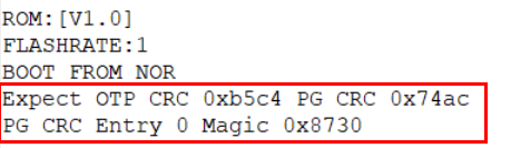
There are 4 CRC entries in total in physical OTP and you can only use one entry at one time. You must use entry 0 first, and then entry1, entry2 and use entry3 at last. CRC check cannot be disabled once enabled. Rom will enter endless loop if magic number or valid CRC check fail.
When you use CRC validation function for the first time, please follow the following steps:
Program CRC entry after you make sure that security zone has been programmed done. Because any modification for the security zone (0x200~0x36B) will cause CRC value changed, then you have to re-program an new CRC entry, which will result in wasting one CRC entry
Get the valid CRC value without actually enabling the CRC function by func:
u32 OTPGetCRC(void)
Program valid CRC value calculated in previous step and magic number (0x8730) of the entry 0.
Magic number is 0x8730:
efuse wraw 370 2 3087
Assuming that CRC value is 0xB4C5:
efuse wraw 372 2 C5B4
Read the CRC entry back, to check whether it’s been written correctly
efuse rraw
小心
Pay attention to the order of data.
Reset the chip
If the CRC entry is checked pass, the boot process will be successfully.
If the CRC entry is checked fail, the following log will show up, and the chip enters endless loop.
If security zone (0x200~0x36B) has been changed, a new CRC entry is needed.
Make sure that security zone has programmed done.
Get the new CRC value.
u32 OTPGetCRC(void)
Program the previous used entry to all 0x00 to invalidate this entry, that means both CRC and magic number are programmed into 0x00.
For example, assuming entry 0 is the previous entry:
efuse wraw 370 4 00000000
Program the next CRC entry with valid CRC and magic number to validate the next entry.
For example, if entry 0 is the previous entry, entry 1 should be used now:
Magic number is 0x8730:
efuse wraw 374 2 3087
Assuming that CRC value is 0xB4C5:
efuse wraw 376 2 C5B4
Read the CRC entry back to check whether it’s been written correctly
efuse rraw
Reset the chip to check if CRC entry is ok.
小心
We suggest users programming CRC entry in factory.
Once CRC entry is programmed, and you need to modify secure zone. Please remember to invalidate current CRC entry and program the correct CRC value and magic number in the next CRC entry before re-boot. Otherwise, chip will enter endless loop and cannot boot successfully again.
隐藏物理区域
隐藏物理区域存储部分 RMA 密钥和 Realtek 校准数据,用户仅可编程与 RMA 相关的区域。
在此区域中,以下两个密钥具备独立的读保护和写保护机制,且会被自动加载到硬件中:
SWD密钥:若处于未编程状态(0xFF),则表明密钥未被启用。
安全启动公钥哈希:若处于未编程状态(0xFF),则表示在 RMA 模式下禁用安全启动功能。
隐藏物理区域的具体内容及用途如下表所示:
Offset |
Bit |
Symbol |
Description |
Usage |
|---|---|---|---|---|
0x700 |
[7:0] |
RMA (Life State) |
Define which mode device works in.
HW will auto-load the work mode first when boot. In RMA mode, the secure 4K bits should be protected and return all |
|
0x701 |
[1:0] |
ROM_PATCH_EN |
Defined by Realtek |
Used by Realtek |
[2] |
ROM_PATCH_LWE1 |
|||
[3] |
ROM_PATCH_LWE2 |
|||
[4] |
ROM_PATCH_LWE3 |
|||
[5] |
ROM_PATCH_LWE4 |
|||
[6] |
ROM_PATCH_LWE5 |
|||
[7] |
ROM_PATCH_HWE |
|||
0x702 |
[0] |
RMA_SWD_PWD_R_Protection_EN |
Key read protection and write protection. |
|
[1] |
RMA_SWD_PWD_W_Forbidden_EN |
|||
[2] |
RMA_PK_W_Forbidden_EN |
|||
[7:3] |
RSVD |
Reserved |
||
0x704 |
[63:0] |
ADC calibration |
Defined by Realtek |
Used by Realtek |
0x710 |
128 |
RMA SWD Key |
SWD Key in RMA Mode |
|
0x720 |
256 |
RMA SBOOT KEY HASH |
SBOOT Key Hash in RMA Mode |
Offset |
Bit |
Symbol |
Description |
Usage |
|---|---|---|---|---|
0x700 |
[7:0] |
RMA (Life state) |
Define which mode device works in.
HW will auto-load the work mode first when boot. In RMA mode, the secure 4K bits should be protected and return all |
|
0x701 |
[1:0] |
ROM_PATCH_EN |
Defined by Realtek |
Used by Realtek |
[2] |
ROM_PATCH_LWE |
|||
[3] |
ROM_PATCH_HWE |
|||
[7:4] |
RSVD |
Reserved |
||
0x702 |
[0] |
RMA_SWD_PWD_R_Protection_EN |
Key read protection and write protection |
|
[1] |
RMA_SWD_PWD_W_Forbidden_EN |
|||
[2] |
RMA_PK_W_Forbidden_EN |
|||
[7:3] |
RSVD |
Reserved |
||
0x704 |
[63:0] |
ADC calibration |
Defined by Realtek |
Used by Realtek |
0x710 |
[127:0] |
RMA SWD Key |
SWD Key in RMA Mode |
|
0x720 |
[255:0] |
RMA SBOOT Key Hash |
SBOOT Key Hash in RMA Mode |
备注
读保护和写保护一旦启用,密钥将无法再次被读取。请务必妥善保管密钥。