Supported ICs
IC |
RTL8721Dx |
RTL8726EA |
RTL8720EA |
RTL8730E |
|---|---|---|---|---|
Supported |
N |
N |
N |
Y |
Introduction
The Liquid Crystal Display Controller (LCDC) is used to fetch display data from main memory and output with MIPI-DSI interface. MIPI-DSI supports several formats, or packet sequences. The following figure illustrates the video mode data transmission.
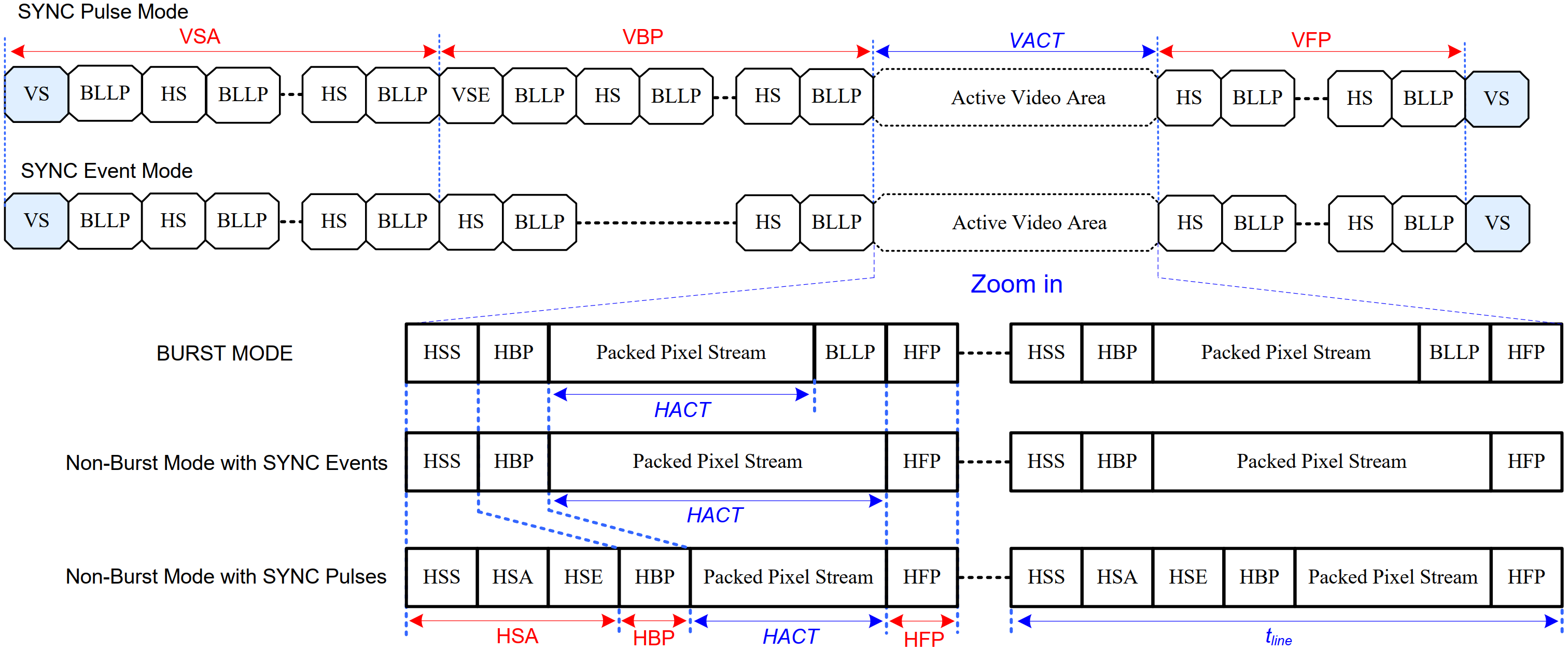
DSI packets
Normally, RGB pixel data is sent with one full scanline of pixels in a single packet. And during the BLLP the DSI Link transmit one or more null packets from the host processor to the peripheral using HS Mode.
When the display function is prepared to be turned on, in order to avoid underflow, the MIPI-DSI must be initialized after the LCDC is ready, so that the LCDC will have enough time to prepare the pixel data of the first line. In contrast, to safely close the display function, stop the MIPI-DSI first and then stop the LCDC.
MIPI-DSI Interface
Display Module Reset Pin
The display module reset pin is _PA_4.
The function Pinmux_Swdoff() needs to be called firstly because _PA_4 is used for SWD by default.
Triggering this pin low enables DSI-CLK+/- lanes and DSI-Dn+/- Data lanes to be driven into Low Power Mode.
Be sure to perform this operation after supplying power if the TFT panels need to be reset.
Command Mode Power Modes
DSI-CLK+/- Lanes
DSI-CLK+/- lanes can be driven into three different power modes:
Low Power Mode (LPM LP-11)
Ultra-Low Power Mode (ULPM)
High Speed Clock Mode (HSCM)
DSI-CLK+/- lanes can be driven to Low Power Mode, when DSI-CLK lanes are entering LP-11 State Code, in three different ways:
After SW Reset, HW Reset or Power On Sequence => LP-11
After DSI-CLK+/- lanes are leaving Ultra-Low Power Mode (ULPM, LP-00 State Code) => LP10 => LP-11 (LPM).
After DSI-CLK+/- lanes are leaving High Speed Clock Mode (HSCM, HS-0 or HS-1 State Code) => HS-0 => LP-11 (LPM).
DSI-CLK+/- lanes can be driven to Ultra-Low Power Mode (ULPM), when DSI-CLK lanes are entering LP-00 State Code. The only entering possibility is from the Low Power Mode (LPM, LP-11 State Code) => LP-10 => LP-00 (ULPM).
DSI-CLK+/- lanes can be driven to High Speed Clock Mode (HSCM), when DSI-CLK lanes are starting to work between HS-0 and HS-1 State Codes. The only entering possibility is from the Low Power Mode (LPM, LP-11 State Code) => LP-01 => LP-00 => HS-0 => HS-0/1 (HSCM).
DSI-Dn+/- Data Lanes
DSI-Dn+/- Data lanes can be driven in different modes which are:
Escape Mode (Only DSI-D0+/- data lanes are used)
High-Speed Data Transmission (DSI-D1+/- and DSI-D0+/- data lanes are used)
Bus Turnaround Request (Only DSI-D0+/- data lanes are used)
These modes and their entering codes are defined in the following table:
Mode |
Entering mode sequence |
Leaving mode sequence |
|---|---|---|
Escape Mode |
LP-11 => LP-10 => LP-00 => LP-01 => LP-00 |
LP-00 => LP-10 => LP11 |
High-Speed Data Transmission |
LP-11 => LP-01 => LP-00 => HS-0 |
(HS-0 or HS-1) => LP-11 |
Bus Turnaround Request |
LP-11 => LP-10 => LP-00 => LP-10 => LP-00 |
High-Z |
Escape commands are illustrated below:
Escape command |
Command type (Mode/Trigger) |
Entry command pattern (First-bit/Last-bit transmitted) |
D1 |
D0 |
|---|---|---|---|---|
Low-Power Data Transmission |
Mode |
1110 0001 bin |
– |
Supported |
Ultra-Low Power Mode |
Mode |
0001 1110 bin |
Supported |
Supported |
Underfined-1 |
Mode |
1001 1111 bin |
– |
– |
Underfined-2 |
Mode |
1101 1110 bin |
– |
– |
Remote Application Reset |
Trigger |
0110 0010 bin |
– |
Supported |
Tearing Effect |
Trigger |
0101 1101 bin |
– |
– |
Acknowledge |
Trigger |
0010 0001 bin |
– |
Supported |
Unknow-5 |
Trigger |
1010 0000 bin |
– |
– |
Video Mode Bandwidth Requirements
Depending on the resolution of the display panel and on the refresh rate, the D-PHY required bandwidth can be calculated below:
BRbps = (VACT+VSA+VBP+VFP) x (HACT+HSA+HBP+HFP) x Pixel Format x Frame Rate/Lanenum
Here, Pixel Format is decided by the packet selected to transmit image data in the MIPI-DSI protocol.
The LSBs are typically dropped once Pixel Format is less than 24bit.
For example:
Frame rate=60Hz
VACT=800Line
VSA=5Line
VBP=20Line
VSA=5Line
VFP=15Line
HACT=480Pixel
HAS=4Pixel
HBP=30Pixel
HFP=30Pixel
Lanenum=2(lane)
Pixel Format=24(bit)
So, BRbps=330Mbps/lane
When image data is transferred to a video mode display module, the MIPI-DSI requests the pixel data from the VO interface.
The pixel data is fixed with RGB888 format, so the result of the frequency of the VO interface multiply by 24-bit shall be great than BRbps x Lanenum to avoid any display problems.
The frequency of the VO interface can be modified to meet the bandwidth requirements of the MIPI-DSI by the CKD_MIPI field of the LSYS_CKD_GRP0 register.
The LCDC required bandwidth depends mainly on three factors:
The number of used LCDC layers
The LCDC layer color depth
The VO Interface clock (depends on the resolution of the display panel and on the refresh rate)
The VO returns 1 pixel data for each VO clock cycle, so the maximum required bandwidth can be calculated as VO_CLK x 3 if three LCDC layers are used and the image layer data format is ARGB8888.
Modifying the CKD_HPERI field of the LSYS_CKD_GRP0 register can change the frequency of LCDC if the bandwidth of LCDC does not meet the requirements of VO Interface. Users should check if the memory bandwidth can sustain the hardware configuration because the master’s concurrent access on the same external memory leads to more latency and impacts its throughput. Setting the LCDC request to HPR can reduce the latency if masters concurrent access DDR Once that the framebuffer location is in the DDR.
How to Use LCDC
To build and run LCDC demo in SDK, follow these steps:
Enable LCDC demo: , and select LCDC_Verify_Mode.
Open the LCDCMIPI clock which is used by VO interface and the HPERI clock used by LCDC.
/*

* @brif   RCC Configuration.
*  by Users.

*/
BOOT_RAM_DATA_SECTION
RCC_ConfDef RCC_Config[] = {
   /*Function,          Clock,                        State*/
   /* AON */
   {APBPeriph_SDM32K,   APBPeriph_SDM32K_CLOCK,       ENABLE},
   {APBPeriph_RTC,      APBPeriph_RTC_CLOCK,          DISABLE},
   {APBPeriph_ATIM,     APBPeriph_ATIM_CLOCK,         DISABLE},
   {APBPeriph_BOR,      APBPeriph_CLOCK_NULL,         DISABLE},

   {APBPeriph_PSRAM,    APBPeriph_PSRAM_CLOCK,        DISABLE},
   {APBPeriph_AUDIO,    APBPeriph_CLOCK_NULL,         DISABLE},
   {APBPeriph_AC,       APBPeriph_AC_CLOCK,           DISABLE},
   {APBPeriph_DDRP,     APBPeriph_DDRP_CLOCK,         ENABLE},
   {APBPeriph_DDRC,     APBPeriph_DDRC_CLOCK,         ENABLE},
   {APBPeriph_IRDA,     APBPeriph_IRDA_CLOCK,         DISABLE},
   {APBPeriph_ECDSA,    APBPeriph_ECDSA_CLOCK,        DISABLE},
   {APBPeriph_ED25519,  APBPeriph_ED25519_CLOCK,      DISABLE},
   {APBPeriph_RSA,      APBPeriph_CLOCK_NULL,         DISABLE},
   {APBPeriph_IPC_HP,   APBPeriph_IPC_HP_CLOCK,       ENABLE},
   {APBPeriph_LEDC,     APBPeriph_LEDC_CLOCK,         DISABLE},
   {APBPeriph_TRNG,     APBPeriph_TRNG_CLOCK,         DISABLE},
   {APBPeriph_USB,      APBPeriph_USB_CLOCK,          DISABLE},
   {APBPeriph_SDH,      APBPeriph_SDH_CLOCK,          DISABLE},
   {APBPeriph_SPI1,     APBPeriph_SPI1_CLOCK,         DISABLE},
   {APBPeriph_SPI0,     APBPeriph_SPI0_CLOCK,         DISABLE},
   {APBPeriph_GDMA,     APBPeriph_GDMA_CLOCK,         ENABLE},
   {APBPeriph_LCDC,     APBPeriph_LCDCMIPI_CLOCK,     ENABLE},
   {APBPeriph_IPSEC,    APBPeriph_IPSEC_CLOCK,        ENABLE},
   {APBPeriph_LX1,      APBPeriph_LX1_CLOCK,          ENABLE},
   {APBPeriph_NULL,     APBPeriph_HPERI_CLOCK,        ENABLE},
Modify
MipiDsi_ST7701S()by your LCM parameter, and in this function LCM is initialized by the following steps:Call
MIPI_StructInit()to define the configuration parameters of MIPI-DSI.Set configuration parameters according to your requirements.
Trigger the display module reset pin low.
Call
MIPI_DPHY_init()to configure the D-PHY.Call
MIPI_DSI_init()to configure the MIPI-DSI.Send init CMD to LCM according to the ST7701S_init_cmd_g[] in command mode.
Call
LcdcRgbDisplayTest()to switch to video mode to start display.Call
LCDC_StructInit()to define the configuration parameters of LCDC.Set configuration parameters according to your requirements.
Call
LCDC_Init()to configure the LCDC.Call
LCDC_CheckLCDCReady()to wait LCDC is ready.Call
MIPI_DSI_Mode_Switch()to switch to video mode for image display.